Contact Us
Thank you! Your submission has been received!
Oops! Something went wrong while submitting the form.
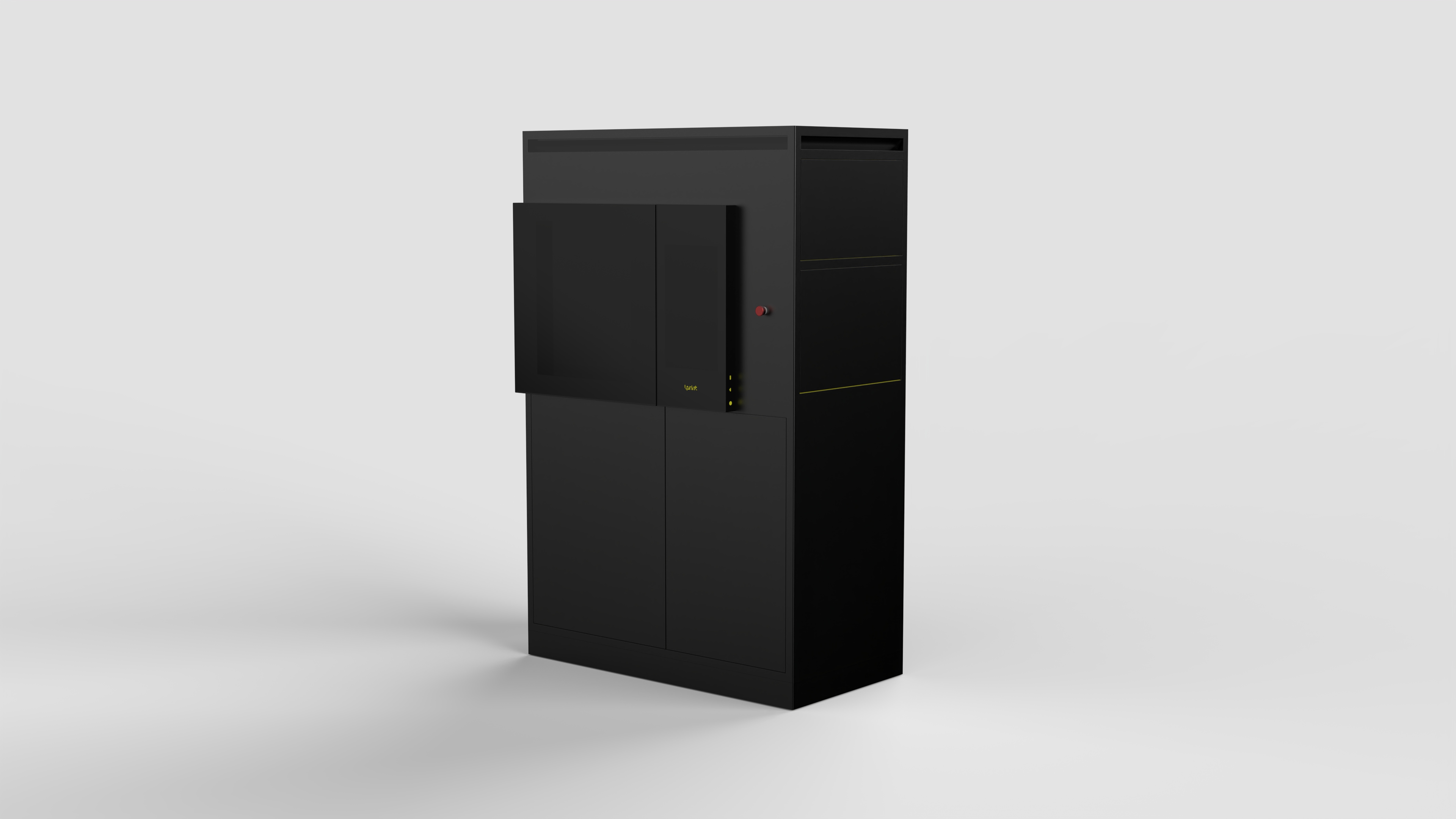
The complete in-house solution for multilayer PCB printing
Our printer and unified software let you load a Gerber file and print PCBs — any geometry, any layer count, right on your bench.
Get samples
>
How it works?
Keep the workflow you already know: design, export, done. With Lprint, that Gerber file goes straight to a 3D printer that delivers a fully functional, multilayer PCB within the same workday.

Ecad Design
Create PCB layout in Altium, KiCAD, Cadence, etc...

Import
Load design files into Lprint’s local software

Print each layer
- Material deposition (conductive or insulating) from cartridges
- Laser sintering bonds layers together

3D modeling, slicing
Software converts files into a 3D PCB model, slices into layers

Get final PCB
Builds up all layers — conductors, vias, insulation — from scratch.

Assemble
Final PCBs drop into your existing soldering or EMS lines


