
Home
Product
Services
Industries
Resources
Company
Contact
FR
English
Français
EN
FR
Menu >
Home
Solution
Industries
Resources
Company
Contact
Français
English
Contact Us
Thank you! Your submission has been received!
Oops! Something went wrong while submitting the form.
News & Q&A
Stay up to date with Lprint’s latest progress and find clear answers to the most common technical questions.
Stay up to date with Lprint’s progress
Thank you! Your submission has been received!
Oops! Something went wrong while submitting the form.
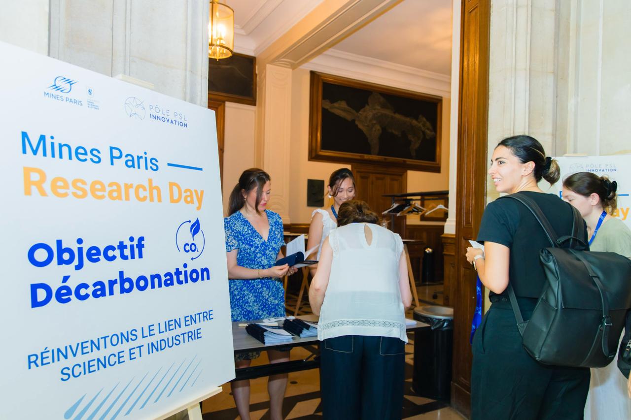
LPRINT at the Mines Paris Research Day 2026
July 2026
We presented at the stand under the Décarbonation track.
Read more
>
Lprint at VivaTech 2026
June 2026
Lprint participated at VivaTech 2026, as part of the Institut Polytechnique de Paris ecosystem.
Read more
>
More articles
>
Q&A
What does the printing process look like from a developer’s perspective?
The PCB design is done in classic ECAD software like Altium, Cadence, etc. The design results in Gerber files. These Gerber files are imported into our software, which recreates a 3D model of the board, slices it into layers for printing, converts these layers into G-code, and sends the G-code to the printer for printing.
How many layers can be printed?
Theoretically, there are no limits.
Where is the start-up headquartered?
The startup is headquartered at the Drahi X-Novation Center at École Polytechnique.
How and when was the company founded?
The company was officially incorporated on May 12, 2025, under the SIREN number 944 185 875. We are currently in the prototyping stage.
Want to get in touch?
Thank you! Your submission has been received!
Oops! Something went wrong while submitting the form.